Chips with everything
These days virtually everything contains semiconductors,” says Dr. Murat Gulcur, Material Development Manager for semiconductors at Trelleborg. “The latest mobile phones have more computing power than big computers of 10 to 15 years ago, maybe even five years ago. We take what’s inside them for granted. We never really think about what is behind our ability to upload a highresolution photo to social media in less than a second, while millions of users are doing the same thing at the same time globally.
“If only 10 percent of all social media users upload just one image a day, imagine how much data needs to be processed and stored,” he continues. “Add email to that, which requires storing and backing up constantly. The amount of data is growing and growing, and in the background all of that is processed using semiconductors.”
The computing power of a microchip or integrated circuit is directly related to the number of transistors it has. Maximizing computing power means that more transistors need to fit on these devices.
“The technology behind semiconductors has evolved significantly over time, particularly around their miniaturization,” continues Gulcur.
“In the very first integrated circuit, there were only 16 transistors with a feature size of 40 micrometers or 40,000 nanometers — about half the width of a human hair.” Gulcur explains that the term “feature size” refers to the size of the elements on a semiconductor.
In 1965, Gordon Moore, co-founder of Intel, said that the number of transistors that would fit on a given area of silicon would double every two years. A few years later he revised his statement, which is now known as Moore’s Law, and said that the number of transistors per integrated chip would double every 18 to 24 months — an astonishing prediction that proved true.
Today’s integrated circuits have billions of transistors, and the manufacturing process is at the nanoscale. The most advanced technology node, or feature size, as of today is down to five nanometers. That is five one-billionths of a meter.
“Moore’s Law has applied up until recently,” says Gulcur, “but in the near future maybe we will finally see the number of transistors in an integrated circuit slowing down. That’s because we are stuck, as the feature sizes are now approaching the physical limits of the space of a semiconductor, and we can fit no more transistors on a chip’s twodimensional surface.”
However, processing power and data transfer speed need to increase further. It is not only required for the devices that we can see and handle but also for recently emerging critical trends that need huge storage and processing capacity, such as autonomous driving, Artificial Intelligence, big data, the Cloud and the Internet of Things.
“Semiconductor engineers are increasing processing power by creating complex architecture in three dimensions to fit more transistors in a unit area,” explains Gulcur. “We are going beyond the realms of traditional physics into quantum physics and mechanics, and the design rules are changing.”
Microchips are manufactured in semiconductor fabrication plants, which are essentially giant cleanrooms with extremely expensive and specialized production equipment. Much of this equipment relies on critical sealing that can stand up to the particularly harsh conditions of fab processing.
“Extending the life of seals is key to lengthening planned maintenance intervals,” says Gulcur. “This can reduce total cost of ownership in semiconductor fabs, but even more importantly it can optimize semiconductor wafer output. Every second counts on high-volume semiconductor production lines. Emergency downtime must be avoided and planned maintenance times minimized.”
At the nanometer scale, air is extremely dirty. In production, everything that is involved in microchip manufacturing, including seals, must be as clean as possible so that no particles enter the semiconductor manufacturing process from outside.
“Particles not visible to the naked eye can lead to defects on semiconductor wafers,” says Gulcur. “It is paramount that seals within semiconductor manufacturing equipment are super clean on delivery to avoid damage to minute electronic components, causing so-called killer defects. Our seals for semiconductor fabrication are therefore manufactured in cleanrooms, from raw material to end product. Until they are ready to ship, our parts never leave the cleanroom and are specially packaged after an intensive cleaning process. This helps our customers increase yields.”
Seals also need to perform effectively in all process steps involved in semiconductor production, and that is more challenging as the process steps increase and process conditions become harsher in fabs.
“Now there are a larger number of process steps to make a microchip,” says Gulcur. “For example, when feature sizes were 28 nanometers, there were about 400 process steps. For a five-nanometer feature size there are thousands, despite advanced extreme ultraviolet [EUV] lithography in high-end semiconductor manufacturing.
“Every process step must take place in a cleanroom,” he says. “Our cleanrooms are clean; at ISO 5/ Class 100, we’ll have a maximum of 100,000 particles larger than 0.1 μm per cubic meter. The semiconductor manufacturers’ cleanrooms are ISO 1, which is 10,000 times cleaner than ours.
“Our seals are in a continual development cycle,” he says. “As the industry changes to meet ever increasing demands for processing power and volume, the challenges for both the microchip manufacturers and us increase.
“Specialist materials that once operated perfectly well are taken to their limits, and we need to develop the next generation of even better materials. To continue to fulfill the requirements of semiconductor equipment manufacturers, we must be continuously alert, not just to keep up with the trends but also to anticipate them and how they will impact our products. We need to be ready to take action.”
Do you know the lingo?
Semiconductor: A type of material that has an electrical resistance adjustable from an insulator to a full conductor.
Semiconductor fab: A semiconductor fabrication plant or foundry.
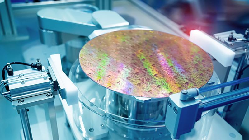
Wafer: The base of all microchips or integrated circuits. A wafer is made of pure silicon crystal with embedded ions to give it semiconductor characteristics.
Microchip or integrated circuit: These are almost the same thing – a bundle of semiconductor devices that consist of multiple circuitry elements.
Feature or node size: The feature or node size is the definition of a semiconductor device size. The smaller the feature size, the more advanced the microchip.
Transistor: A semiconductor circuitry element that switches or amplifies an electrical signal. In computers, transistors are mostly used as switches. Transistor arrays are used for storing data as memory and doing computation in binary mode.
This is an article has been reproduced from Trelleborg's T-Time magazine. To download the latest edition, go to: www.trelleborg.com/t-time