The Fab Four


gives us information about the booming semiconductor sector and introduces the new Isolast® PureFab™ range.
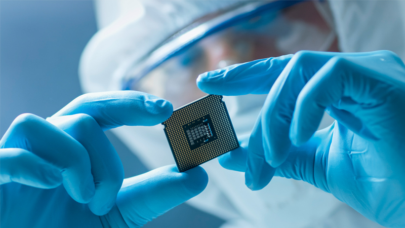
SEMICONDUCTORS ARE INTEGRAL TO ALMOST ALL THE ELECTRICAL AND ELECTRONIC EQUIPMENT
that we use in our daily lives. They are fundamental to our computers and mobile phones, but they are also behind other less obvious applications, such as the advanced functions in our cars and even creating shopping lists from our fridge.
Growing market
The history of these little pieces of magic dates to 1947, when a group of engineers at Bell Labs in the US, made the first transistor. The original integrated circuit (IC), which consists of numerous transistors on a single ‘chip’ of silicon, was made by Texas Instruments in 1958. In 1960, the first metal oxide semiconductor (MOS) was produced by engineer Jack Kilby.
In just 60 years, the semiconductor industry has grown to a power house that will generate, according to Statista, just over 433 billion US dollars in sales worldwide in 2020.1 Stimulated by the booming innovations in Artificial Intelligence in all sectors, as well as 5G, autonomous driving, the Internet of Things and Big Data, by 2022, PricewaterhouseCoopers predicts that the market will be worth 575 billion US dollars.2 Fortune Business Insights projects it to reach over 730 billion US dollars by 2026, exhibiting a compound annual growth rate of 5.2% from 2019.3
The state-of-the-art manufacturing techniques and facilities of Trelleborg Sealing Solutions help make product designs a reality. We’ve invested in the latest manufacturing technologies to provide the most advanced solutions, which bring optimized product designs to the semiconductor market.
Decades of experience have led us to develop new and improve existing methods for producing innovative and reliable products. In particular, these include leading edge micro-molding technology, cleanrooms and our unique FlexiMold™ process.
Continual miniaturization
The technology behind semiconductors has evolved significantly over time, particularly around their miniaturization. In 1965, Gordon Moore, co-founder of Intel, said that the number of transistors that would fit on a given area of silicon would double every two years. A few years later he revised his statement, which is now known as “Moore’s law”, and said that the number of transistors per integrated chip would double every 18-24 months; an astonishing prediction that has so far proved right.
In the very first integrated circuit, there were only 16-transistor chips with a feature size of 40 micrometers (40,000 nm), about half the width of a human hair. On today’s ICs there are billions of them, which are smaller than 10 nm, or a hundred millionth of a millimeter.
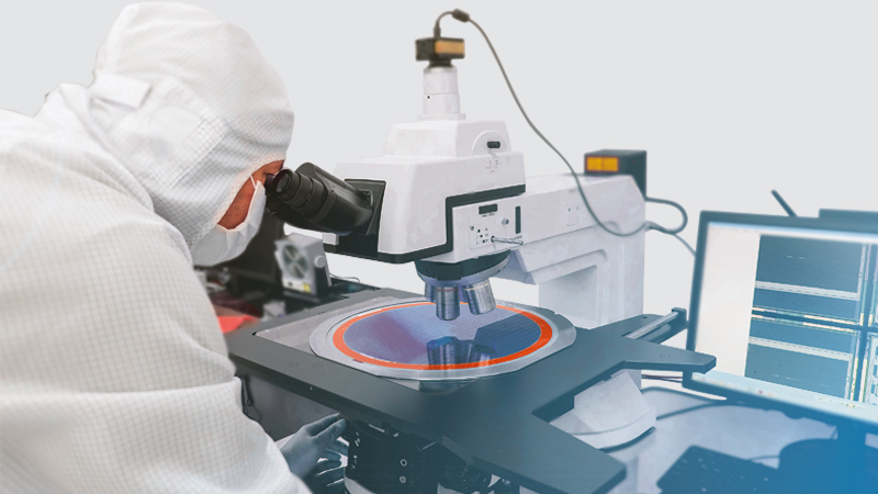
Microchips are manufactured in semiconductor fabs, which are essentially giant cleanrooms with extremely expensive specialized production equipment. Much of this equipment relies on critical sealing that can stand up to the particularly harsh conditions of fab processing. It is paramount that seals do not shed particulates or generate gases during operation, as this would cause damage to minute electronic components, so called killer defects.
Extending the life of seals is key to lengthening planned maintenance intervals. This can reduce total cost of ownership in semiconductor fabs, but even more importantly,
optimize wafer output. Every second counts on these high-volume production lines, and emergency downtime must be avoided.
Challenging requirements in difficult sealing environments
The manufacturing process behind semiconductors has been down to the nanoscale for some time and is now pushing the boundaries of physics, with the most advanced technology node as of today down to 5 nm, just above the width of a hemoglobin molecule, with 3 nm on the horizon. At this scale, purity, cleanliness, and minimum contamination are vital to microchip manufacturing, as transistors continue to be miniaturized and each wafer is packed with hundreds of billions of them.
Particles that cannot be seen by the naked eye can lead to defects on wafers. Spotting the source of contamination and cleaning the wafers can cause significant loss of time at the front-end of the semiconductor manufacturing process. Moreover, metallic impurities in parts per billion (one billionth of a gram) can change the electrical properties of a wafer and therefore cause dysfunctional microchips.
Another factor that increases the challenge in semiconductor sealing, is that, unlike other industries, such as aerospace and oil & gas, there are no standards for sealing that are widely used. This is mainly because each chip manufacturing fab has its own process conditions and gasses optimized for its own products. Requirements for sealing materials are therefore very different and there is no ‘one size fits all’ solution.
FFKM becomes the only solution
Extreme temperatures and chemicals used in harsher processes mean only perfluoroelastomer (FFKM) can stand up to process environments. FFKMs have the elasticity
of an elastomer and very similar chemical resistance to a Polytetrafluoroethylene (PTFE) material.
We’ve always had a strong range of semiconductor options in our Isolast® PureFab™ FFKM range. Recently we decided to expand our offering and have developed four market leading materials that are completely in line with today’s and more importantly, the developing needs of tomorrow’s fabs. The new leading-edge materials address the requirements of some of the most difficult sealing environments created by semiconductor manufacturing processes, whether it is in plasma, extreme high temperatures or the destructive chemicals in wet processes. Sealing in plasma processes was a particular challenge when it came to material development.
Plasma resistance
Plasma is an ionized gas consisting of positive ions, radicals and free electrons in proportions resulting in no overall electric charge, typically at low pressures, as in the upper atmosphere, stars, and fluorescent lamps. It is widely used in semiconductor processes for etching or activation of chemicals.
FFKM base polymers are fully organic, and therefore their plasma resistance is very low. To improve this, a lower erosion ingredient - usually fillers - is blended into the FFKM formulation; filler particles shield the polymer matrix from plasma exposure, hence improving the plasma resistance of the material.
Various types of fillers can be used in FFKM formulations. Each one of them has some advantages and disadvantages over the others, therefore it is crucial to select the correct sealing material for each specific semiconductor process.
Fully organic solutions
Organic fillers provide higher purity and better particle performance and therefore less contamination. The FFKM polymer and organic fillers form gaseous molecules when they are exposed to plasma. These gaseous substances can be pumped away by a vacuum, meaning these materials provide a very clean processing environment.
Part of our development process for the new semiconductor materials focused on trying to engineer a material that operates effectively in plasma using organic fillers. This resulted in Isolast® PureFab™ JPF10, which is one of the best performing fully organic materials on the market. It provides the sealing characteristics required by the highly demanding semiconductor processes to manufacture the most advanced microchips.
The benefit of a fully organic composition is that the material has an unrivalled low level of particle generation and excellent outgassing performance, increasing process yields
and lowering the total cost of ownership of semiconductor processes. It offers excellent high temperature sealing performance and purity.
In some highly critical semiconductor processes, the requirements of a sealing material can be even more stringent. For example, if a process node is below 10 nm even higher purity may be needed if the elastomer part is in close proximity to the wafers. To maintain volume wafer output, a specially formulated ultra-pure FFKM translucent material without any filler may be required.
In these situations, Isolast® PureFab™ JPF30 can meet extreme purity requirements while offering unrivalled high temperature performance and sealing integrity compared to other translucent FFKM materials in the market.
At Trelleborg Sealing Solutions, we support our customers in the global semiconductor industry with innovative solutions designed to accelerate their business by maximizing yield and minimizing overall cost of ownership.
We do this by forming lasting partnerships with customers to design, prototype, manufacture & deliver unique, high-performance engineered polymer solutions for the most demanding semiconductor applications.
We combine cutting edge, high purity materials with established advanced engineering capabilities to deliver superior performance & service for our customers.
Find out more about these new leading-edge materials by going to www.tss.trelleborg.com and downloading our flyers on these innovative compounds.
Isolast® PureFab™ is the Trelleborg Sealing Solutions brand for its proprietary range of semiconductor materials, which provides extreme purity and performance. The compounds undergo significant testing to prove their properties. Additionally, all parts are manufactured, cleaned, and packaged in cleanrooms to avoid contamination by particles from the outside world.